Introduction
iFixit is proud to present the Sony PSP Go teardown once again! Enjoy. Also check out the YouTube video slideshow!
What you need
-
-
Oh joy! Oh joy! Guess what we got our hands on this time! Its the brand spanking new Sony PSP Go!
-
Although the design of the PSP Go is different from previous PSP models, the PSP Go is not intended to replace its much loved older brother, the PSP 3000.
-
-
-
Such an elegant backside... But where is the UMD drive? Let's have a moment of silence. R.I.P. UMD drive, we hardly knew ye.
-
The PSP Go measures at 128 x 16.5 x 69 mm and weighs in at 5.6 oz (including the internal battery).
-
Unlike previous PSP models, the PSP Go makes do with 16 GB of internal flash memory.
-
Oooooh it slides up to reveal the gamepad!
-
The product label has the usual power requirements and FCC warnings. It appears even Japanese companies have their products manufactured in China.
-
-
-
Removing the necessary screws required to gain access into the innards of the PSP Go.
-
On this device, all screws are readily accessible and use a common Phillips #0 head. No hidden tabs or tri-wing screws here.
-
With a non-soldered battery and Phillips head screws, why doesn't Sony approve of DIY battery replacement?
-
We can think of only one reason: it starts with "cha," and ends with "ching." That's right, the sound of the cash register.
-
-
-
A simple flick of a PSP opening tool and presto!
-
Ladies and Gentlemen, behold! The inside of the PSP Go.
-
Unlike the Zune HD or the iPod Classic, the Go uses no metal internal framework. In fact, it has no internal framework; all structural integrity is provided by the plastic outer cases.
-
-
-
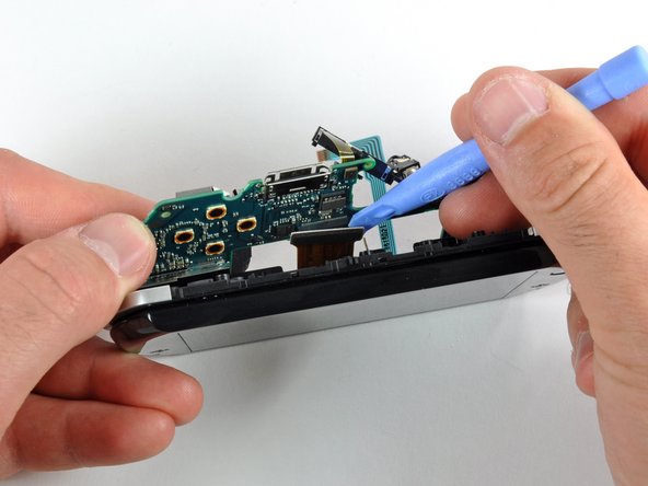
We begin our dissection by disconnecting a few connectors and removing a couple screws.
-
It was clear the board wouldn't come out without first removing the triggers. So we decided to start with the left trigger button.
-
The trigger button ribbon cables are connected to the board with ZIF connectors; a careful flick with the PSP opening tool released the clamp and freed the ribbon cable.
-
-
-
Firmly stuck to the battery is a trilingual Warranty Void seal. They really covered all bases with this one, as long as you know English, French, or Spanish.
-
Good news: the battery is not soldered to the board.
-
Bad news: unfortunately, you have to peel the warranty sticker back to remove the battery.
-
But more good news: if you're careful, you can remove the battery without disturbing the "VOID" portion of the seal, but we didn't tell you that.
-
Just slide a PSP opening tool in between the battery and sticker. Work your way gently side-to-side, until the battery is free from the sticker. Presto-changeo!
-
-
-
-
The battery's a Li-ion 3.7V, 930 mAh, 3.5Wh unit.
-
Here's how the three major handheld gaming devices stack up in the battery department:
-
PSP Go: 930 mAh, unofficially user replaceable
-
DSi: 840 mAh, officially user replaceable
-
iPod touch 3rd Gen: 789 mAh, unofficially user replacable, requires difficult soldering
-
The PSP wins on capacity, and the DSi wins on serviceability. The touch, well, if you can't say something nice...
-
-
-
With the board out, we can continue tearing into the Go.
-
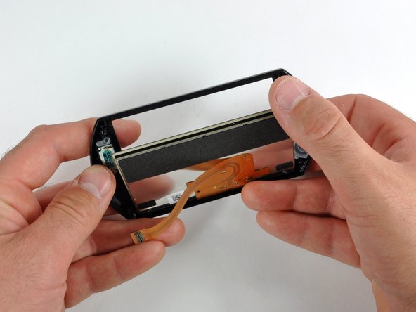
A couple screws must be removed to separate the display assembly from the lower case.
-
With the lower case and logic board gone, you can see the details of the metal slider mechanism. That display ribbon cable must be designed for wear from millions of opening/closing cycles.
-
-
-
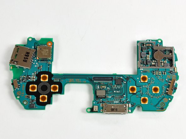
The backside and the frontside of the PSP Go logic board, with joystick still attached.
-
Now we will turn our attention to identifying the many chips that make the Go... well... go.
-
The sheer number of chips and EMI covers is amazing. The device certainly has a large number of dedicated-function chips, as opposed to having a few large multi-tasking chips.
-
-
-
The first picture includes:
-
SHARP 0923 7y LR388G1 TFT-LCD controller for video out.
-
OKI L86V7657 9175902J
-
The second picture is of the QZ7-001A 95D ALPS 002433 A73457 Bluetooth communication chip.
-
For the third picture:
-
SCEI 923KMO3 4053
-
U3031 9M93
-
The small object highlighted in green on the third picture is the surface mounted microphone.
-
-
-
And there you have it: the Go in pieces.
-
Curious how the PSP stacks up the the handheld gaming competition on the inside? We have both a DSi teardown and an iPod touch teardown.
-
Be sure to keep an eye on our teardown page for an inside look at the latest gadgets!
-


5 Comments
Is there a way to remove the start & select buttons on the GO? If so can some add pictures on how to do this. Thanks in advance.
I'd say you can follow this guide and just push the buttons out of the front case.
Is there anyway to connect a umd drive from any of the other PSP preferred 1000 as I am planing to making a PSP console hopefully from a PSP go as this has the Bluetooth in it to connect a ps3 controller I know you may think it's pointless but it's something I like to do
What are the psp go's tft screen pinouts?