Introduction
Anxious to have the Galaxy S 3 in the palm of your hand? Join us as we take an exciting sneak peek at the Samsung Galaxy S III, the appropriately-named successor to the Galaxy S II. Images provided courtesy of Chipworks!
Follow iFixit on Twitter if you're keen on getting the latest updates on our teardowns!
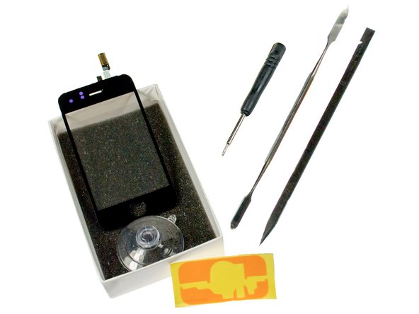
What you need
-
-
First, let's give thanks where thanks are due: a big, solid, awesome thanks to Chipworks for providing the pictures for this teardown. We greatly appreciate their help for the Samsung Galaxy S III!
-
Here's their full analysis on the Galaxy S III.
-
-
-
Arguably the most hyped-up Android phone to ever hit the market, the Samsung Galaxy S III has an impressive list of accolades. Here are some of the heavy-hitting tech specs:
-
Android 4.0 Ice Cream Sandwich
-
4.8" Super AMOLED 720 x 1280 resolution display
-
1.4 GHz quad-core application processor
-
2100 mAh battery
-
8 MP rear-facing and 1.9 MP front-facing cameras
-
16, 32, or 64 GB of internal storage
-
Pictured here next to the Samsung Galaxy S2 (left) for comparison.
-
-
-
The simple, sleek design of the newest Galaxy S implements a standard power/sleep button on the side of the device.
-
As we ready ourselves to dig into this Galaxy S, it watches us with its rear 8 MP camera. To the left and right of the camera are the flash and speaker assemblies.
-
The Galaxy S is not only watching us, but listening, as well.
-
-
-
Much like in the Galaxy Nexus, we find a user serviceable battery in the Samsung Galaxy S III.
-
The 3.8 V, 2100 mAh battery incorporates the antenna for the Near Field Communications (NFC) module used in "S Beam".
-
For those who are curious, 2100 mAh is equivalent to 7560 Coulombs of charge. Unsurprisingly, this is the same amount of charge that a 3.8V, 7.98 Wh battery holds.
-
-
-
Internals time. The spudger takes care of the first two plastic assemblies.
-
The first piece out is the rear plastic frame that protects the motherboard and houses a single liquid indicator sticker.
-
Removal of the frame grants us access to an easily replaceable speaker assembly.
-
-
-
-
We continue by removing the motherboard from the inner framework.
-
With the motherboard out of the way, we can get a good look at the inner support frame. While we suspect that the frame is probably magnesium, we do not yet have any concrete proof.
-
We find a chip that isn't attached to the motherboard: a Melfas 8PL533 Touch Sensor that translates your touch inputs into zeroes and ones.
-
-
-
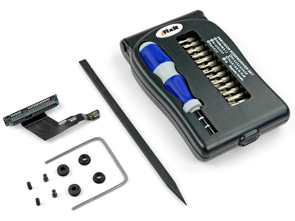
Let's talk tools for a minute.
-
We don't just make awesome teardowns—we sell parts. And tools! Lots and lots of tools.
-
Like this handy-dandy electronics tool kit that we used to take apart the new iPad. You know you want one. It'll pay for itself the first time you use it!
-
We sell Mac parts & upgrades, parts for iPhone screen repair, kits for fixing the infamous Xbox Red Ring of Death, and tons more.
-
We need your support to continue building the free repair manual for everything in the world.
-
-
-
Chipworks eagerly provided us with pictures of the motherboard less than an hour into the teardown! Here is the front of the motherboard:
-
Murata M2322007 WiFi Module
-
Samsung Exynos 4412 quad-core A9 processor with 1 GB LP DDR2 Green Memory (K3PE7E700M-XGC2)
-
Samsung KMVTU000LM eMMC(16GB)+MDDR(64MB) NAND Flash
-
Intel Wireless PMB9811X Gold Baseband processor
-
MAX77693 and MAX77686
-
Broadcom BCM47511 Integrated Monolithic GNSS Receiver
-
33ODC 2214 4TP AC
-
-
-
Bottom of motherboard:
-
Wolfson Microelectronics WM1811 stereo codec
-
Skyworks SKY77604 Multi-Band Power amplifier
-
Silicon Image 9244 low-power MHL Transmitter
-
NXP PN544 NFC Chip.
-
Infineon PMB5712 RF transceiver
-
-
-
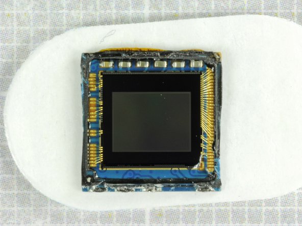
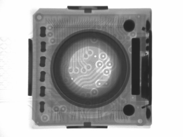
Some more shots of that saucy camera, including a Chipworks x-ray!
-
Chipworks report that the camera has a Sony BSI sensor. Contrary to earlier reports, their initial inspection suggests it is a new sensor, and not the same one used in the iPhone 4S. The bond pad arrangement is not the same as the IMX145 found in the iPhone 4S nor is it the same as the IMX105 found in previous Samsung phones.
-
-
-
Update: This teardown was conducted solely via Interweb, requiring us to defer judgment on a repairability score. Now that we've worked on it ourselves, we can assign it a fair score:
-
Samsung Galaxy SIII Repairability Score: 8 out of 10 (10 is easiest to repair)
-
The battery can be replaced without any tools.
-
Very easy to open and access internal components.
-
There are only 12 screws in the entire device, all standard Phillips #0 (no proprietary or security sizes).
-
Smaller components (antennas, vibrator, light sensor) are modular and can be replaced individually, but are adhered to the front panel.
-
The glass is fused to both the display and the display frame, increasing repair costs.
-
You'll have to go through the entire phone in order to replace the front panel, since everything is built into the back of it.
-


29 Comments
can you guys do a teardown of the Sprint one so we can know if the LTE SIM card is soldered in or simply covered by the plastic?
why is there STILL no repair score?