Introduction
We had so much fun tearing down the iPhone 5s and 5c, that we just couldn't stop. We've got the tracks laid for a teardown of Apple's new A7 processor. Head over to the station 'cause the teardown train is chuggin' along. The next stop: Science.
Lucky for us, we've got Chipworks as our steadfast engineers on this trip. We're piling on the coal for one wild ride through the internals of this lightning-fast chip.
All aboard!
Whether you're riding the rails, pulling the caboose, or tied to the tracks, hitching your wagon to iFixit on Instagram, Twitter, and Facebook will keep you on track.
-
-
It's that time of year again. The air is crisp, the leaves are turning, the Apples are coming out. If you ask us, the best thing about fall is tearing into an Apple or two. In the spirit of the season we're headed into Apple's A7 processor.
-
It wouldn't be Apple season without our friends at Chipworks. Thanks to these bearers of good tidings, we have the inside scoop on Apple's new processor.
-
-
-
What, you wanted to see the internals?
-
Don't worry, we'll get there. But first, here's the science behind the magic.
-
It's not science without a laboratory. And Chipworks has just that.
-
We've got total ion blaster envy for Chipwork's Ion Beam Etcher, or IBE.
-
Our friend IBE takes layers off a semiconducter by blasting it with atoms in an ion beam. Power. Precision. Prettydangawesome.
-
-
-
After pre-processing the chips are examined. It's best to see that your specimen is ready...
-
...ready for the transmission electron microscope (TEM).
-
This bad boy is handy when you want to know transistor strain, gate oxide thicknesses, or crystal lattice orientation.
-
Like the ion blaster, the TEM uses the shoot-first-ask-questions-later method by blasting electrons at its prey to see just what they're made of.
-
We've had fun taking a tiny peek at Chipworks's playground, but we've got to move on before the anticipatory drool leads to a series of keyboard replacements.
-
-
-
As promised by Apple, and most recently confirmed by Gizmodo via the magic of benchmark testing, the A7 provides twice the performance of the A6 processor.
-
The A7 is the first use of a 64-bit processor in a smartphone. Based on AnandTech's review, it seems that the bulk of the A7's performance gains do not come from any advantages inherent to a 64-bit architecture, but rather from the switch from the outdated ARMv7 instruction set to the newly-designed ARMv8.
-
-
-
With the help of fancy, expensive equipment, Chipworks produced a die photograph of the A7. It looks a lot like its predecessor, the A6.
-
Early on, our good friends at Chipworks had this to say about the A7:
-
“We have confirmed through early analysis that the device is fabricated at Samsung’s Foundry. We suspect we will see Samsung's 28 nm Hi K metal Gate (HKMG) being used."
-
You'd think they'd just stop at the die and call it good, amirite?
-
Amiwrong.
-
-
-
-
Check out the A7 processor's cross-section. Every little hump (through which you see that yellow line) is a transistor. By measuring the total distance between ten of these transistors, we can estimate a chip’s manufacturing process—essentially how tightly the manufacturer can pack in all that processing power.
-
The techs at Chipworks took out their [nano]meter stick and measured the distance between these transistors, which at first seemed very similar to the A6.
-
But wait! It turns out that the A7′s “gate pitch” — the distance between each transistor — is 114 nm, compared to the A6′s 123 nm.
-
Those 9 nm are a big deal. Looking to improve on their current 32 nm process, Apple decided to make the A7 with the same 28 nm process as the eight-core Samsung Exynos 5410, the current flagship CPU for Samsung’s own Galaxy line.
-
So what does that translate to? Applying some mathematrickery (28^2 divided by 32^2 = 784/1024), this seemingly small change equates to having the same computing power, but in 77% of the original area. And given that the A7 processor is larger in area than the A6, that means even more processing power to lead a healthy, smartphone-laden lifestyle.
-
-
-
The A7 transistor level die photo reveals all one billion plus transistors on a 102 mm2 field.
-
No, don't bother getting out the magnifying glass, we'll up the zoom a little more for you.
-
Update: Our chip-buddies have given us the "floorplan" of the A7!
-
-
-
Chipworks did some investigatin' and found the M7 to be an NXP LPC18A1, part of the LPC1800 series of high-performing ARM Cortex-M3 based microcontrollers.
-
Don't believe them? Check out the NXP inscription in the top right of the die photo.
-
From Chipworks: "The M7 is a new direction for Apple: in an effort to reduce power consumption, the M7 chip is dedicated to collecting and processing accelerometer, gyroscope and compass data."
-
-
-
So the M7 is tasked with accessing information from three sensors, and with Chipworks' help we found these too:
-
Bosch Sensortech BMA220 3-axis accelerometer
-
STMicroelectronics 3-axis gyroscope
-
AKM AK8963 3-axis magnetometer
-
Using the A7 to monitor this sort of data would be mega-overkill, so the M7 was introduced to maintain a constant, low-power watch over these sensors.
-
-
-
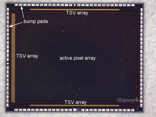
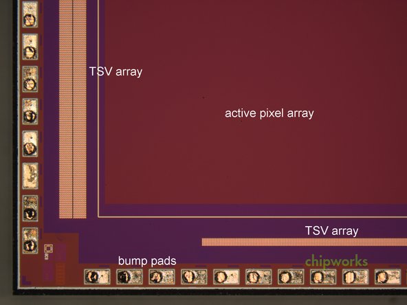
This time around, Apple opted to stick with 8 MP resolution for the iSight camera, but increased the active pixel array area by 15%. Bigger pixels and a wider f/2.2 aperture means the system delivers a 33% increase in light sensitivity.
-
That's gravy and all, but ever wonder what a 1.5 µm pixel pitch actually looks like? Well wonder no more! The first image in this step shows how your camera sees you when you take that duck-faced selfie.
-
-
-
Contained within this module is the BCM4334, like we saw last year in the iPhone 5. It includes IEEE 802.11 a/b/g/n single-stream MAC/baseband/radio, Bluetooth 4.0 + HS, and an integrated FM radio receiver.
-
It is designed to be used with external 2.4 GHz and 5 GHz front-end modules, which include power amplifiers, T/R switches and optional low noise amplifiers.
-
Apple chose not to upgrade the iPhone to the latest Broadcom chipset to take advantage of their new 802.11ac base stations.
-
-
-
The Qualcomm MDM9615M 4G LTE modem utilizes a two-chip system: a Samsung-fabricated LTE baseband processor paired with a Samsung DRAM module to retain carrier specific information.
-
-
-
With all of the power of the new A7, exciting camera features, and the M7 coprocessor, it's easy to forget that smartphones are still phones, and making and taking calls ought to be a pretty high priority. This functionality is handled by an impressive array of RF components working together:
-
Skyworks SKY77810 2G/EDGE Power Amplifier
-
Avago A792503 Band 25/3 Power Amplifier
-
RF Micro RF3763 Band 5/8 Dual Power Amplifier
-
Skyworks SKY77572 Band 18/19/20 Power Amplifier
-
Skyworks SKY77496 Band 13/17 Power Amplifier
-
TriQuint TQF6414 Band 1/4 Dual Power Amplifier
-
-
-
Thanks for joining us on this tour of electronic discovery, and a big thanks again to our friends at Chipworks!
-
For the in-depth scoop, be sure to check out Chipworks' article, Inside the iPhone 5s.
-
And if you missed them last week, don't forget to check out our teardowns of the iPhone 5s and iPhone 5c, still hot and fresh from the land down under.
-


-02.jpg)
10 Comments
Above the GPU blocks, there appears to be an sRAM block to my eyes. That's interesting, as the Wii U GPU also has that on the GPU die in addition to its larger slower eDRAM. I wonder what the performance implications are, and how big that is. I wonder if it could be used for the framebuffer for the GPU, or if it serves another function? It's too far from the CPU to seemingly be related to that. Too much latency for no reason.
Maybe it's for security. XBOX 360 CPU has a sRAM block to store the hypervisor, memory encryption keys and other security stuff so the most essential security process never leave the chip. Maybe this has to do with the "secure enclave" apple talks about.
Tom Chai -
Actually no. FM radio chip comes with the wifi/bt chip, they are sold as one package at least since iphone 4s. But Apple has no plan to ever use it. so the pins for FM radio are simply not connected. I have the circuit schematic. solid proof
Tom Chai -