
This teardown is not a repair guide. To repair your ASUS ZenPad S8, use our service manual.

  1. ASUS ZenPad S8 Teardown, ASUS ZenPad S8 Teardown: step 1, image 1 of 2 ASUS ZenPad S8 Teardown, ASUS ZenPad S8 Teardown: step 1, image 2 of 2
    • ASUS ZenPad S8 outside

  2. ASUS ZenPad S8 Teardown: step 2, image 1 of 1
    • The back case didn't use any screw or glue. The back case only use tenons to stick with front case. It's not hard to take apart.

  3. ASUS ZenPad S8 Teardown: step 3, image 1 of 3 ASUS ZenPad S8 Teardown: step 3, image 2 of 3 ASUS ZenPad S8 Teardown: step 3, image 3 of 3
    • There are three big parts in tablet-- upside circuit board, battery and downside circuit board. Base on my experience, upside circuit board has more important IC chips than downside board.

  4. ASUS ZenPad S8 Teardown: step 4, image 1 of 3 ASUS ZenPad S8 Teardown: step 4, image 2 of 3 ASUS ZenPad S8 Teardown: step 4, image 3 of 3
    • Let's closer look at the upside circuit board. We found 4 important IC chips.

    • Hynix 4GB LPDDR3 DRAM.

    • Intel Atom Z3580.

    • Kingston eMMC 32GB NAND Flash

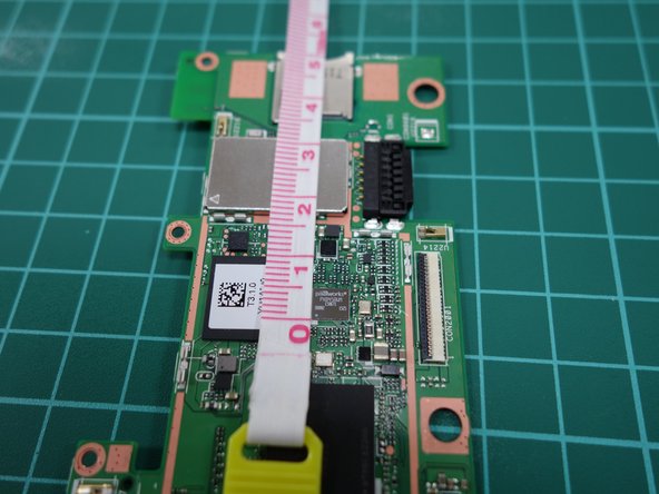
    • Pixelworks PX8458WM. This is the independent high-end TV level video processor I'm looking for!!!

  5. ASUS ZenPad S8 Teardown: step 5, image 1 of 3 ASUS ZenPad S8 Teardown: step 5, image 2 of 3 ASUS ZenPad S8 Teardown: step 5, image 3 of 3
    • Let's measure the size of Pixelworks IC. It's about 5mm x 5mm (0.2inch x 0.2 inch)

    • From Pixelworks CEO comment, we know ASUS ZenPad S8 use IRIS1 chip. Although IRIS1 chip also target on smartphone market, we didn't find any smartphone use IRIS1 chip yet.

    • When I ask ASUS tablet PM about the possibility of IRIS1 on smartphone, he imply the power consumption level of IRIS1 may not reach smartphone requirement. It will be more reasonable to see IRIS1 on tablet or laptop.

Ken

Member since: 11/20/13

273 Reputation

1 Guide authored

View Statistics:

Past 24 Hours: 1

Past 7 Days: 14

Past 30 Days: 27

All Time: 24,071