Introduction
A destructive insight into the hardware involved in letting the iPad talk to SD cards.
What you need
-
-
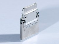
The iPad camera connection kit. A accessory that many feel does something the iPad should already do.
-
Anyways, here is it torn to pieces (literally), in the interest of seeing what is involved in letting the iPad, which only has a serial and USB interface, talk to a SD Card.
-
-
-
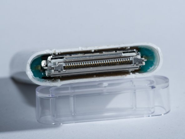
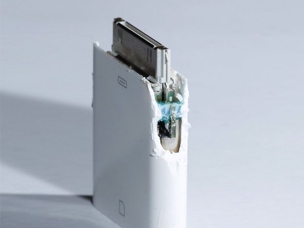
The first step is to even determine how the adapter was assembled, since it has no visible screws.
-
The grey plastic surrounding the dock connector seems to be an insert. Some aggressive prying with a metal spudger caused it to come loose, but not without significantly damaging the plastic housing itself.
-
-
-
-
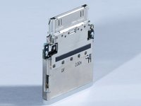
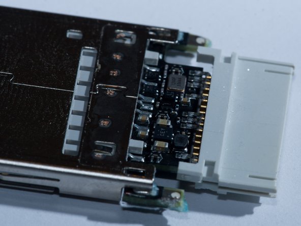
With the casing removed, we see... More barriers!
-
The Circuit board is protected by a metal EMI shield, which is liberally spot-welded in place.
-
This thing is utterly un-repairable. It seems it is designed in the same manner as the magic trackpad, and many of Apple's other recent pieces of small hardware.
-
-
-
Onward! Spot-welds are generally fairly brittle, and these welds are not very strong, since a truly penetrating weld would likely heat the metal to the point where the plastic parts would melt.
-
Therefore, by forcefully prying, the spot-welded metal components apart, it is possible to break the welds.
-
-
-
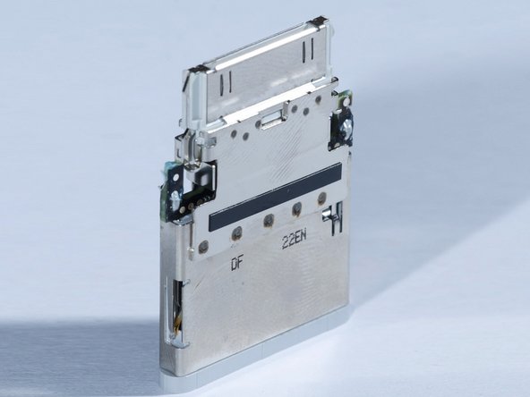
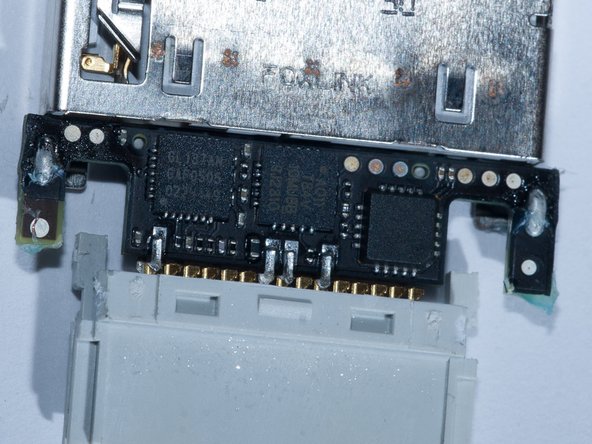
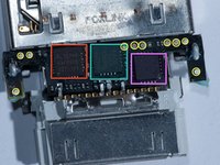
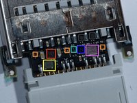
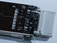
Finally, the circuit board revealed!
-
considering the size of the board, there is a lot of hardware packed on to it.
-
GL137AN GAF0505 022H149 - In a 28 pin QFN package
-
A011 T84V 10MUBB 9J2310 - In a 20 pin QFN package
-
2257 AE072 90K - In a 20 pin QFN package of different origin.
-
Assorted 0402 and 0201 passive components.
-
Testpoints, complete with visible divots from probing during manufacture.
-
-
-
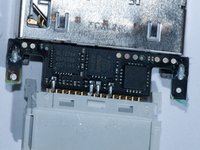
Finally, the bottom of the interface board. Of interest, what appears to be a small DC-DC converter of unknown purpose. The iPad only supplies 3.3v. For the USB camera connection adapter, a DC-DC converter is required to provide the 5V to run USB devices. However, SD cards run natively on 3.3v, leaving the purpose of the DC-DC a mystery.
-
Tiny package marked only with patterned dots, likely for computer recognition.
-
Little tiny SMT inductor. Unmarked.
-
CEY and some dots. Location near inductor leads to it being likely it is the DC-DC converter IC. 6 Pin package.
-
94F5LF - Very small package, Likely BGA.
-
ET ZD - 4 Pin Package.
-
1200P E06AA - Almost certainly a canned clock oscillator. Probably some permutation of 12 MHz.
-
3 Small 6 pin packages. Pin arrangement leads me to believe they are ferrites or some sort of filter. Probably part of power supply
-