Introduction
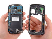
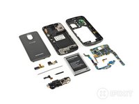
It's here, it's here, it's finally here! The sun is shining, the birds are chirping, and the ice cream truck is driving up the street, playing its joyful tune. We have our dollars ready, and we can't wait to grab ourselves some goodies. Join us as we unwrap our favorite frozen treat, the Ice Cream Sandwich-laden Galaxy Nexus.
Interested in getting the inside scoop on the latest teardowns? Follow us on Twitter!
What you need
-
-
The Galaxy Nexus packs some serious hardware inside. Key specs include:
-
1.2 GHz Dual-Core Processor
-
1 GB RAM
-
16 GB Internal Storage
-
4.65" Super AMOLED Display
-
5 MP (1080P HD) Rear-Facing Camera
-
Near Field Communication (NFC) and Wi-FI Direct
-
Android 4.0 Ice Cream Sandwich
-
-
-
Like most of Samsung's smartphones, the Galaxy Nexus' 5.0 megapixel camera is perched in the middle of the phone's backside.
-
"Clean" is the word that comes to mind as we look at the rear of the Galaxy Nexus. You won't find any "1080p HD" markings or model numbers here.
-
Just like the Nexus S, the Galaxy Nexus features a Contour Display. The curved glass conforms to the side of your face and makes talking on the phone more comfortable.
-
Maybe, some time in the very distant future, phones will become so advanced that they fit perfectly to the user's ear and mouth.
-
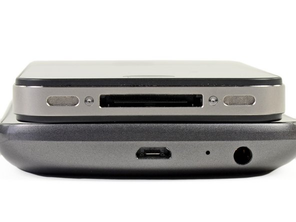
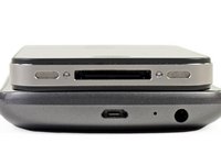
The power button and three gold pins for multi-media docking occupy the starboard side of Google and Samsung's flagship smartphone.
-
-
-
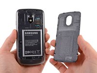
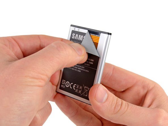
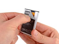
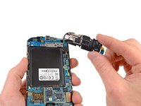
Not only does the 3.7 V, 1750 mAh battery power the phone, but the user manual states that it also doubles as the NFC antenna.
-
O RLY? We had to see this one for ourselves.
-
Lo and behold, there's a sweet antenna hiding underneath the battery's shiny wrapper. So if you ever want to buy a replacement battery (and keep NFC functional), ensure that the battery has the antenna.
-
-
-
Tool used on this step:iFixit Opening Picks (Set of 6)$4.99
-
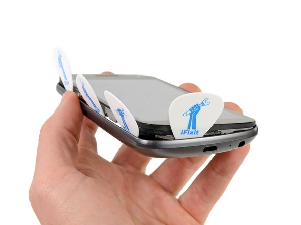
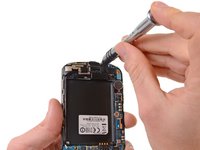
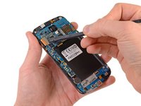
Whipping out our handy 54 Bit Driver Kit, we reach for a Phillips #0 bit and get to work opening the phone.
-
We wrenched our plastic opening tool till it was blue in the face and went through more guitar picks than Jimmy Page, but we managed to take off the back case. No device is too tough for the dexterous hands of the iFixit crew!
-
-
-
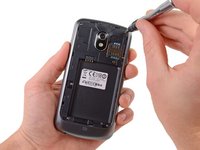
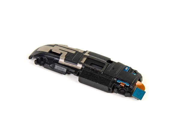
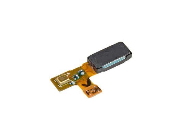
One little screw shackles the speaker and headphone jack assembly to the motherboard.
-
Goodbye, little screw; hello, speaker and headphone jack assembly.
-
With access to Google Music and high definition movies, there's no doubt that Galaxy Nexus owners will want their phone to make some beautiful noise. Unfortunately, our disassembled phone didn't make a single chirp.
-
-
-
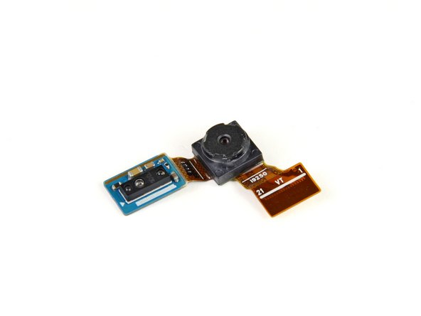
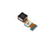
A flick of the spudger and out come the front- and rear-facing cameras.
-
The 5 megapixel rear-facing camera is optimized for low light conditions and has a handy continuous auto-focus feature that'll surely help keep those quick moments clear. If you prefer moving pictures, this camera can capture full HD 1080p "talkies."
-
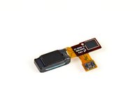
The front-facing camera allows for video chat and will take pictures at 1.3 MP or videos at 720p.
-
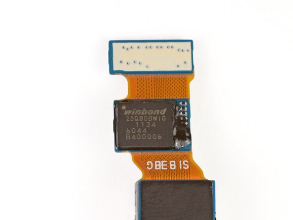
The rear-facing camera has a Winbond 8 Mb Serial Flash Memory unit in line to help it buffer all the data it collects.
-
-
-
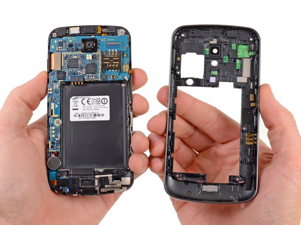
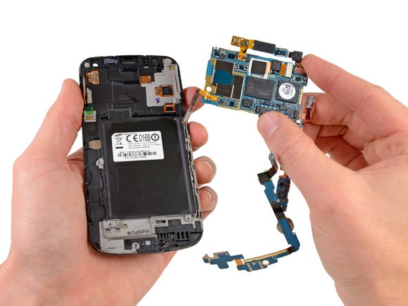
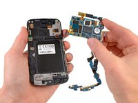
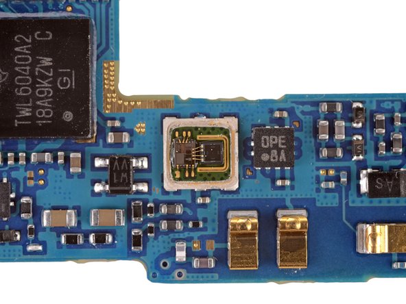
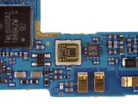
The primary internals of the Galaxy Nexus are held on two L-shaped boards. The small board on the left holds the vibrator motor and several connections. The large board on the right is the motherboard, which houses the volume buttons, SIM slot and the following chips:
-
Texas Instruments TWL6040 8-Channel High Quality Low-Power Audio Codec
-
Texas Instruments TWL6030 Fully Integrated Power Management with Switch Mode Charger
-
Invensense MPU-3050 Motion Processing Unit
-
Intel XG626 Baseband Modem
-
Bosch BMP180 MEMS Pressure Sensor
-
-
-
Flipping both boards over reveals a lot of nothing on the smaller board, but a ton of chips on the motherboard—a "smörgås-board," if you will:
-
RFMD RF6260 Quad-band Multimode Power Amplifier Module
-
Samsung KMVYL000LM Multichip Memory Package, which we believe to house 512 MB of RAM in addition to the main processor.
-
Samsung K3PE7E700M 512 MB DDR2 SDRAM
-
Samsung SWB-B42 BT 4.0 Dual Band Wlan FM Tx/Rx. Chipworks says the module is actually manufactured by Murata, and houses a Broadcom BCM4330 die inside.
-
NXP 65N00 Smart Card IC. According to Chipworks, this two-die package houses an MCU and a PN544 NFC controller.
-
Silicon Image 9244 MHL transmitter
-
SiRF SiRFstarIV GSD4t GPS tracker
-
-
-
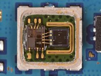
The chip labeled as 274 U141 031 hides the Bosch BMP180 MEMS Pressure Sensor, which should be responsible for the "Barometer" feature inside the Nexus.
-
Check out the wire bonds on the third image. This is a very, very small chip.
-
Just how small is it? Well, here's how a U.S. dime looks like next to the chip (indicated by red arrow)
-
-
-
A Melfas 8PK173 1126 Touch Screen Controller allows users to control the Galaxy Nexus with "...fun, consistent gestures."
-
-
-
Samsung Galaxy Nexus Repairability Score: 6 out of 10 (10 is easiest to repair).
-
Battery replacement is incredibly simple thanks to the removable rear panel.
-
Minimal adhesive makes removal of the motherboard and other components a snap.
-
Headphone jack and speaker assembly are not soldered to the motherboard, so replacement is easy.
-
The only soldered components are the volume switch and vibrator motor.
-
Removing the rear case to access the motherboard and other internals requires a lot of careful prying and guitar-picking.
-
The glass is fused to both the display and the display frame. So don't crack the glass unless you're good with a heat gun, or you're fond of replacing the glass, display, and frame together ($$$).
-


31 Guide Comments
We are pretty sure that the rest of the memory is contained in the Multichip Memory Package.
According to Samsung: http://www.samsung.com/us/business/oem-s... the K3PE7E700M-XGC1 is a 1GB LPDDR2 memory package.
According to ABIResearch: http://www.abiresearch.com/research/1008... the KMVYL000LM MCP houses 16GB of NAND flash and only 64MB of SDRAM.
The OMAP4460 is almost certainly underneath the K3PE7E700M-XGC1, not the KMVYL000LM. I tried to make these corrections but those changes were denied. Apologies if that is not allowed here. Let me know how I can help get the correct information there.
Alex,
We always appreciate user contribution and input! You have pointed out an interesting conflict between the Samsung part specification (which has a slight part number mis-match) and the ChipWorks identification. Samsung claims 8 Gb and ChipWorks claims 2 sets of 2Gb totaling 4 Gb. Based on our discovery of ChipWorks claim of 4 Gb, we were under the impression that ABI had a typo (they are not a well known source to us). As far as location of the processor, we only make our guesses. Because we didn't de-cap any of the chips this round, we can not make any solid statements about the processor's location. We will certainly be investigating the memory conflict and making changes if we are SURE that a change is necessary. We always appreciate reader input, so please keep on reading!
Actually, there isn't a part number mismatch with Samsung's catalog. Samsung just listed the part number in a confusing way. The catalog lists "K3PE7E700M-XG(1)", but the "(1)" isn't actually part of the part number, it's a footnote below the table, which says that the "(1)" stands for two letters that designate the speed. Since this particular part is LPDDR2, the corresponding designation is "C1". So the part number in its entirety is "K3PE7E700M-XGC1", which is exactly the part we are looking at. Since this is an exact match, we can be pretty confident that this is an 8Gb module, and ChipWorks made an error in their listing.
As for the location of the SoC, I'm just going by what ChipWorks has said in the past with their analysis of devices that also happen to use the K3PE7E700M, but I understand that you don't want to speculate without further verification. Are you planning to de-cap the chip in the future? Many of us are curious whether the OMAP4460 has distinguishing marks compared to the 4430.