Introduction
We partnered with Chipworks to bring you a teardown of the all-new Microsoft Kin Two!
The Microsoft Kin Two is the Kin One's taller brother, and is manufactured by Sharp Electronics.
What you need
-
-
-
The top of the phone features a headphone jack, while a Micro USB port can be found on the bottom.
-
The Kin Two is 19.05 mm thick. That makes for a bigger bulge in the pants, given that the thickness of the iPhone and Motorola Droid are 12.3 mm and 13.7 mm, respectively.
-
Enter "Is that a Kin Two, or are you happy to see me?" jokes here.
-
-
-
Sliding the screen upwards reveals a relatively simple keyboard. No fancy D-pad, just one "alternate" text button. Judging from the look of the keyboard, Microsoft's marketing this phone to the 12-year-old txting crowd.
-
The back side reveals the lovely 8MP camera and LED flash...
-
...And the back cover comes off to reveal several screws underneath!
-
It looks like it's pretty easy to exchange the battery in the Kin Two. Hint, hint, Apple!
-
-
-
With the two sliding halves of the phone separated, you can easily see the odd-shaped springs that keep the phone either fully open or fully closed.
-
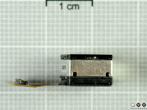
The connector highlighted in yellow is responsible for sending data between main board and the display, microphone, speaker, and touchscreen.
-
Several rows of pressure contacts help exchange data between the main board and the external buttons, microphone, speaker, and antennas embedded in the outer case.
-
-
-
The camera is the Sony IMX046, which is fabricated using a 90 nm CMOS process. The camera's resolution is 8.11 effective megapixel (8 active megapixel), 1.4 μm sized pixel, 1/3.2" optical format. Samsung was the first to use this camera in the M8800.
-
An LED flash placed next to the camera lens on the rear case sheds some light on night shots.
-
For all its pixels, the camera only eats up about .5 cm3 of space inside the Kin.
-
-
-
-
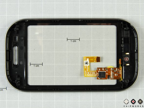
Separating the two halves of the display assembly reveals a bunch of cables connecting the microphone, speaker, display, and digitizer to the main board.
-
-
-
The digitizer is a Synaptics unit, and the main controller chip is labeled T1021A 1 0939 ACOM755.
-
-
-
The front and back of the main board.
-
The camera is nestled quite nicely in a little cutout near the top of the board.
-
When buttons are pressed on the QWERTY keyboard, they simply bridge the connection between the gold ring and its center dot.
-
If only the steel shield supports were gone so we could view the board unobstructed...
-
-
-
Texas Instruments' TPS-6586 Advanced Power Management Unit controls power onboard the Kin and takes care of charging its lithium battery.
-
-
-
The Wolfson Micro WM8903 is a low power stereo codec with all sorts of fancy features like programmable audio path control sequences, both pseudo-differential and fully-differential analog inputs, a dynamic range controller, and all sorts of other technical jibber jabber.
-
-
-
Was ist das? It's actually an Nvidia Tegra processor, buried beneath an Numonyx package seen on the surface.
-
Samsung's moviNAND chip supplies the 8GB of storage space for the Kin.
-
The moviNAND package can transfer data at speeds up to 52 MB/s.
-
The Qualcomm QSC6085 package delivers up to 1.8 Mbps reverse and 3.8 Mbps forward speed on CDMA-2000 networks.
-
-
-
The small silicon chip pictured appears to be a Texas Instruments WL1271 for WLAN and possibly Bluetooth connectivity.
-
Avago's ACFM-7103 PCS/Cellular/S-GPS Quintplexer simplifies mobile applications designed for simultaneous voice service and GPS positioning.
-
Another Avago chip, the ACPM-7353, provides dual band power amplification for cellular and PCS connectivity.
-
-
-
STMicroelectronics LIS331-DL inertial sensor (3-axis digital MEMS accelerometer).
-
Another chips near the camera connector were not readily identifiable, but they most likely help with transferring data between the camera and the main board.
-
AKM's AK8973 3-axis Electronic Compass. The same like in most mobile devices today. Placed out of the shield to feel geomagnetic field freely.
-
We'll update the teardown as we find out more. Follow @ifixit to stay up-to-date with the hardware world.
-
Thanks again to our friends at Chipworks for the photos!
-