
You may have noticed we have a fair number of device X-rays on our site lately. Be it wallpapers, teardown photos, or just quick tweets, Creative Electron has been providing us (and you!) with top-quality imagery for years now. While we usually post some individual analysis of their rich black-and-white findings, we can’t always fit all our intel into a teardown step or tweet. So it’s time to empower you to do your own X-ray analysis. That’s right—this is an X-ray x-plainer.

X-rays are a form of electromagnetic radiation outside the visible spectrum that can penetrate objects. By aiming X-ray waves through objects, we can capture imagery of device internals. Like any other kind of photography, the X-ray “light” hits a sensor and captures an image with it. The denser a material is, the fewer X-rays pass through it, and the darker it appears in the image. That principle enables doctors to see breaks in a bone, and for us to see gaps in electronics.
Bill Cardoso, CEO of Creative Electron, says, “I’m always amazed by the range of applications that use X-ray inspection. One day we’re looking for cracks on a helicopter blade, next we’re looking for defects on a golf ball. From checking the viability of seeds to assessing the quality of iPhones, X-rays are used daily to make our lives better.”
Manufacturers may be looking for defects. We’re looking for features, trying to get a pre-teardown sneak peek at components, and maybe some guidance on where we should start prying or heating to get inside. All we have to do is look for familiar shapes while keeping density in mind!

First off, density alone can tell you a lot, mostly about the material used. Context, gained from examining similar devices, tells you the rest of the story.
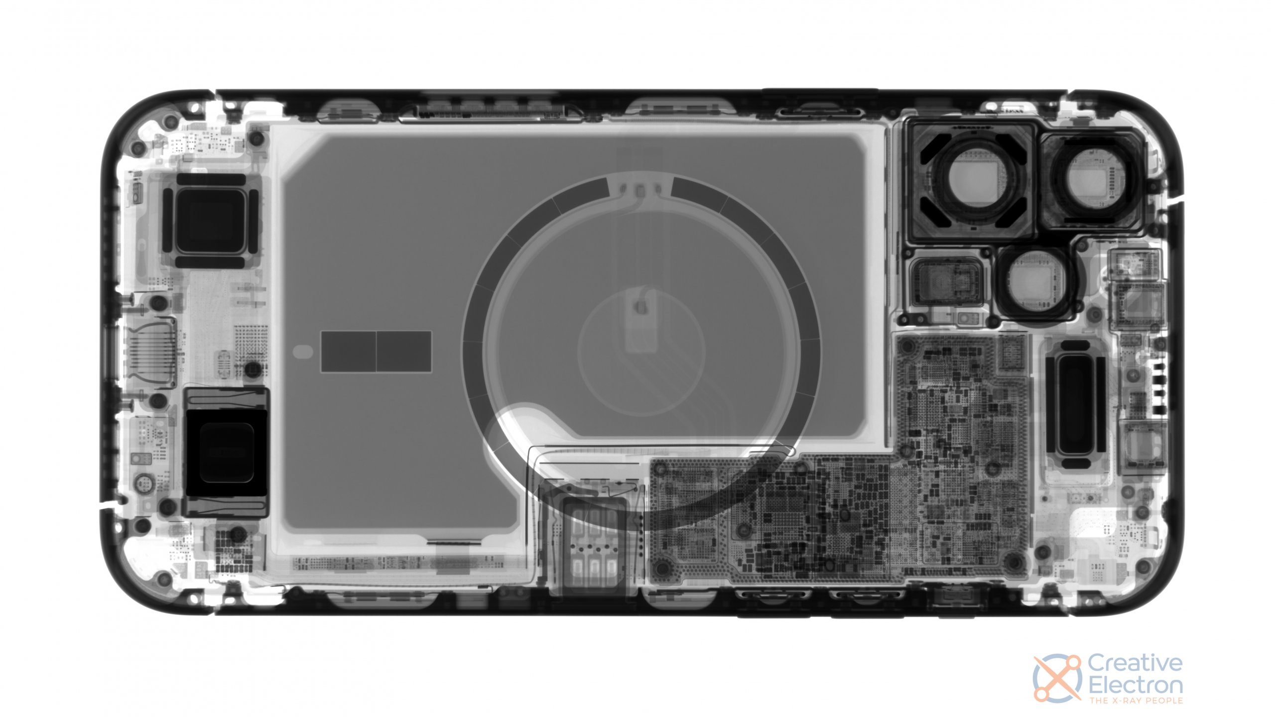
You can see in the above image of a Pro-model iPhone 12 that it’s surrounded by a pretty dark outline—especially compared to non-Pro models. That’s steel! The Pros use a dense, strong material to give their larger phones bend-resistance, and, we’d guess, a premium heft.

If you’ve got small dark areas, they’re often magnets. Small, dark squares near a camera? Probably optical image stabilization (OIS). OIS uses electromagnets to keep the image sensor steady while your wibbly wobbly hands shoot pictures. Large dark patches near the top and bottom of the phone are often the earpiece and loudspeakers.
Rounded rectangles, a.k.a. “chiclets,” are usually case magnets, often used for aligning accessories. Tablets like the Surface Pro, and iPad, use them to attach smart cases with built-in keyboards. The “smart” part comes into play when a Hall Effect sensor registers the position of a magnet, usually dimming or waking a display as you close and open the case. The 12-series iPhones use a ring of magnets to help align to their wireless charging pads, increasing charging efficiency.

A grid of dark gray circles? Probably a surface-mounted chip! The series of dots is what’s called a ball grid array (BGA) since it’s well… a grid of balls of solder. You may have heard of this mounting method from its famous failures, such as Touch Disease and game console Rings/Lights of death.\

Got a mix of dark and light? Pull out your birding component matching guide, and let’s get to spotting!

Small surface-mount capacitors feature dense, dielectric darkness, but still look like their slightly-pinched-breadloaf selves. Resistors aren’t very dense at all and can be hard to see, but can be spotted by the solder that holds them to their boards.

iPhone 11 Smart Battery Case 
Apple Watch Series 0 Display
Concentric rings are usually inductive (i.e. “wireless”) charging coils. NFC antennas also come in concentric form, but inductive charging coils are usually larger and denser. That being said, the two are sometimes integrated into a single assembly, as in the iPhone.

How about a bonus round? Sometimes you face something new and it takes some visible light (and actual opening) to properly identify it. But next time, you’ve got one more data point. Take the Apple-specific Taptic Engine, a linear oscillator in a steel enclosure. It shows up dark on an X-ray, similar to a speaker, but the zig-zag of springs gives it away.
We’ve only scratched the (dense) surface of X-ray analysis, but now you’re a little wiser, and a little better at spotting teardown tidbits. If you’d like to play along and identify components yourselves, we’d love to see what you spot in our teardown comments! You can also find Creative Electron on the socials, or read their in-depth blog posts! Otherwise, catch you next teardown!


0 Comments