Introduction
Our Kindle 2 shipped on Monday, February 23rd, a day early. Thanks to UPS Next Day Air, we have the reader in our hands Tuesday morning.
What you need
-
-
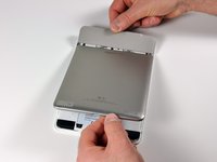
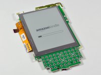
It's here!
-
Thanks to the magic of E-Ink, the Kindle comes with setup instructions displayed on the screen itself. No plugging in is required.
-
-
-
Size comparison: Definitely not as big as a 17" MacBook Pro Unibody.
-
The Kindle 2 weighs only 10.2 ounces. Per pound, that makes the Kindle 2 even more expensive than the $2,799 MacBook Pro 17" Unibody we took apart last week.
-
-
Tool used on this step:Metal Spudger$2.99
-
Prying the back off...
-
Getting inside is easy once you know how. We used some plastic opening tools and a metal spudger, and finally managed to get in.
-
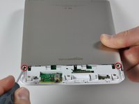
The matte-gray top cover comes off first.
-
There are two Phillips screws to remove before the Aluminum back can be removed entirely.
-
-
-
-
Remove two Phillips screws and the battery lifts out easily.
-
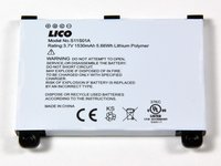
The battery is Model No. S11S01A. It's a 3.7 V, 1530 mAh lithium polymer battery. The battery weighs in at 31 grams, just over 10% of the Kindle's total weight.
-
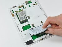
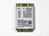
The wireless card is also easily removable by removing two Phillips screws.
-
-
-
After removing sixteen more screws, we've made it to the main PCB.
-
Everything exciting is still beneath silver EMI shields.
-
The Kindle was designed by Lab126, a secretive Amazon subsidiary based in Cupertino that designs consumer devices. Thus far, they have only released the Kindle 1 and 2.
-
-
-
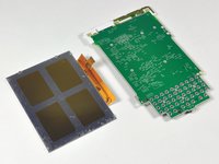
Even with the battery completely removed, the screen displays a crystal clear image.
-
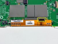
The display is held by a "window frame" of adhesive. Gentle prods and twists from all sides with a plastic opening tool separated the display.
-
Removing the display reveals a bunch of vias on the PCB. Nothing too terribly exciting.
-
-
-
A close-up shot of the center area of the board.
-
The large MC13783VK5 is a Freescale battery power management chip.
-
The ISP1105 (smaller chip in the left enclosed area) is a USB transceiver.
-
-
-
The main processor is in the upper left. The Freescale chip is labeled MCIMX31LVKN5C M91E CTAH0850V. It's a 532 MHz, ARM-11 90nm 14mm package.
-
To the right of the processor, the Samsung K4X1G323PC is a 32MB mobile DDR SDRAM chip. There another Samsung SDRAM chip in the lower right.
-
The large Samsung package in the lower left is the Kindle's main memory. It's a 2 GB moviNAND package, which includes both flash memory and the cotroller.
-
The co-branded Epson and E-Ink chip on the right is the display controller. It is a PFBGA package that supports "high speed screen updates (2048x1536 at 50Hz+)."
-


5 Guide Comments
hey guys great post. Any idea how or where I can get a HIgh resolution image near the USB connector. I think I knocked off a capacitor or resistor for the kindle 2 model from Lab26 model D00701, just looking to put the part back on but need to confirm the location
since there are other NO LOADs (parts that are not populated).
thanks, Phil
anyone?
For anyone still looking for this, make sure you see my comment under Step 5 for how to properly get the back covers off.